P4x-040

Highlights
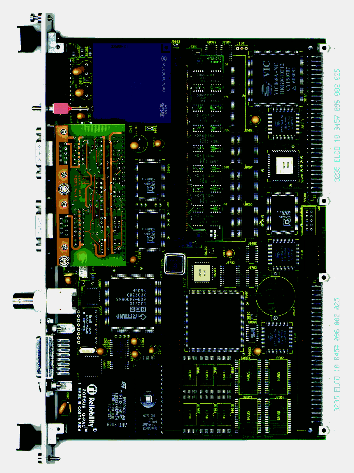
The "P4X 040 system" is a 6U VMEbus
board build around the Motorola MC68040 microprocessor.
It is ideal for high-end embedded real-time
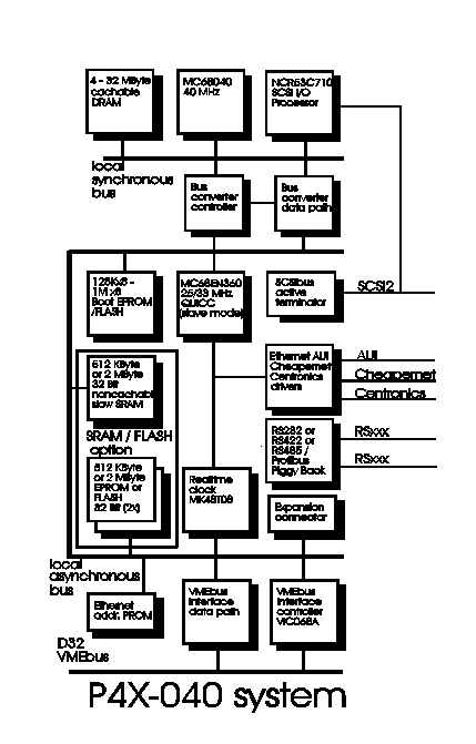
monitor, control and server applications. The usage of the MC68EN360 QUICC as
intelligent multiple IO controller provides a large offering of interfaces:
Ethernet, parallel port, three serial ports configurable as RS232, RS422, second
ethernet or Profibus. The VMEbus interface uses the VIC068A gate array to
provide a complete state of the art backplane transmission media. Mass storage
devices can be handled by the onboard intelligent fast SCSI-2 controller. A key
feature of the P4X is its double local bus structure which permits to each
component to work at its optimum throughput level.
The combination of the high performance
MC68040 and the IO versatility of the QUICC puts low cost features into a high
performance single board VMEbus computer.

Features
- 32 bit microprocessor MC68040,
integrated FPU, MMU, 4 KB data and 4 KB program cache
- clock rate : 80 Mhz (40 Mhz synchronous
bus clock rate)
- main memory :
- 72 pin standard SIMM socket for up to
32 Mbyte dynamic ram modul
- EDO DRAM controller
- byte parity (optional)
- accessible from the VMEbus
- 8 bit fast SCSI-2 bus interface with 32
bit synchronous bus DMA and intelligent SCSI SCRIPT processor
- bus structures :
- synchronous bus for main memory and
SCSI DMA operations with maximum throughput
- asynchronous bus for peripheral and
VMEbus operations
- bus converter for transparent cycle
translation between the two local busses
- MC68EN360 Quad Integrated Communications Controller
(QUICC) used in slave operation mode providing timers, ethernet, serial and
parallel ports
- Ethernet AUI port or cheapernet
interface
- three serial ports configurable as
RS232, RS422, second ethernet and Profibus via serial piggyback module
- Centronics compatible parallel interface
- 32 bit, 512 Kbyte or 2 MByte SRAM bank
with battery backup
- two 32 bit, in circuit programmable
flash memory banks with 512 Kbyte or 2 Mbyte capacity each
- 8 bit wide JEDEC socket for eprom or
flash memory
- 8K x 8 NVRAM and time-of-day clock with
battery backup
- 64 Byte PROM containing a unique
ethernet address
- VIC068A VMEbus interface gate array and
CY7C964 data and address path companion chips providing a complete
state-of-the-art VMEbus interface
- local asynchronous bus expansion
connector for mezzanine card
- 10 LED indicators for function and error
monitoring
- reset and abort switch on front panel
- easy connection of SCSIbus, printer and
remote reset switch via J2 backplane connector
VMEbus Interface
The "P4X 040 system" VMEbus interface has
been optimized for operation in a multiprocessor environment. By using the
VIC068A gate array, more than just the standard VMEbus functions are supported.
One of these additional features is the message passing mechanism which allows
together with the main memory slave capability the efficient implementation of
multiprocessor systems.
The VIC068A chip supports all standard data
transfer modes of the VMEbus as master and slave interface. Additionally 32 bit
block transfer is supported. The write posting feature provides a major relief
of the cpu or the bus master. Data that has to be transferred via the VMEbus is
buffered in fast latches and, afterwards, transferred without any further
interaction of the cpu - any unnecessary cpu cycles are avoided.
The "P4X 040 system" has a software
configurable VMEbus interrupter and interrupt handler module. The following
parameters may be selected : priority of an interrupt request, and the number
and priority of any interrupt request to be handled. This way every possible
interrupt structure may be applied, either a distributed or a central interrupt
system.
The board is able to assume all functions
of a VMEbus system controller : generation of the system clock, reset function,
watchdog timer, iack daisy chain driver, and four level arbitration (single
level, priority, round robin).
Peripheral Interfaces
The 8 bit fast SCSI interface may be used
to connect up to seven mass storage devices (hard disks, optical disks tapes,
and floppy disks). The bus is controlled by the 53C710 chip. The risk kernel
contained in this component allows hardware independent programming by the SCSI
SCRIPT language. The cpu load gets reduced, since the 53C710 relieves it from
controlling the SCSIbus protocol.
The communication channels are implemented
using the Motorola MC68EN360 / QUICC controller chip.
The QUICC delivers the ethernet / IEEE
802.3 protocol on the first SCC channel. An external manchester encoder is
installed on the board.
The "P4X 040 system" offers two different
network media interfaces :
- AUI attachment unit interface for
connection of an external transciever (via DSUB15)
- 10BASE2 thin ethernet (also called
cheapernet) via BNC connector
The P4X has three serial ports which may
configured with different line driver types by means of a serial piggyback
module.
Actually five piggyback options are
available :
| first channel (SCC2) |
second channel (SCC3) |
third channel (SCC4) |
designation |
| RS232 |
profibus
(isolated RS485) |
- |
P4XSP1 |
| RS232 |
RS232 |
- |
P4XSP2 RS232
option |
| RS232 |
RS422 |
- |
P4XSP2 RS422
option |
| RS232 |
RS232 |
Second
Ethernet AUI |
P4XSP3 |
| RS232 |
RS232 |
RS232 |
P4XSP4 |
The standard delivery is with two RS232
ports installed.
In order to connect a printer, a centronics
compatible parallel interface is provided.
The local asynchronous bus is routed to the
mezzanine board expansion connector.
An M-module carrier board can be plugged
into this slot to permit the construction of compact controller systems without
loading the VMEbus.
Manufacturing quality
The SimTech products are
manufactured using high quality components. Each board is submitted to a 12
hours burn in.
Technical
specifications
Main processor
- 32 bit microprocessor Motorola MC68040,
integrated FPU, MMU, 4 KB data and 4 KB program cache
- clock rate : 80 Mhz (40 Mhz synchronous
bus clock rate)
Main memory
- 72 pin standard SIMM socket for up to 32
Mbyte dynamic ram module
- 1M x 36, 2M x 36, 4M x 36, 8M x 36 PS2
compatible modules may be used
- byte parity (optional)
- EDO DRAM controller
- accessible from the VMEbus
IO
processor
- Motorola MC68EN360 Quad Integrated Communications
Controller
(QUICC) used in slave operation mode providing timers, ethernet, serial and
parallel ports
- clock rate : 25 MHz
Static
RAM
- One 32 bit bank of battery backed low
power static ram.
- The total data capacity is 512 Kbytes or
2 Mbytes..
- The data is held during power down with
a lithium type accumulator.
- The typical backup time is 3800 hours
(160 days).
Flash
memory
- Two banks of 32 bit wide flash memory.
- total capacity of 512 Kbytes or 2 Mbytes
per bank.
- 5V operation for read, write and erase.
- minimum of 100 000 write/erase cycles.
Boot
eprom
- A conventional JEDEC compatible 32
socket is available for use as boot eprom.
- The following memory chips can be used :
| Designation |
type |
bit capacity |
byte capacity |
| 27C010 |
EPROM |
1 M |
128 K
|
| 27C020 |
EPROM |
2 M |
256 K
|
| 27C040 |
EPROM |
4 M |
512 K
|
| 29F010 |
5 V
FLASH |
1 M |
128
K |
| 29F040 |
5 V
FLASH |
4 M |
512
K |
- The flash memories are in circuit
programmable with +5V only supply for read, write and erase.
VMEbus (IEEE STD 1014)
- VIC068A VMEbus interface gate array and
CY7C964 data and address path companion chips
- DTB master : A16-A32, D08-D32, BLK
- DTB slave : A16-A32, D08-D32, BLK
- arbiter : RR/PRI
- interrupt handler : IRQ1-7
- interrupt generator : level 1 to 7
- system controller : yes, jumperable
- interprocessor communication support
including four global mailbox interrupts, four module mailbox interrupts and
five mailbox registers
- master and slave write posting
SCSIbus
- controller : 53C710
- 8 bit fast SCSI-2 bus interface
- 32 bit synchronous bus DMA
- intelligent SCSI SCRIPT processor
- active termination
- device connections via J2 backpanel
P4XBP
Ethernet
- controller : SCC1 on QUICC
- 64 byte prom containing unique ethernet
address (also available as system ID)
- manchester encoder : AM7992B
- AUI port DB15 female connector on front
panel
- cheapernet transciever : AM7996
- isolated 10BASE2 BNC connector on front
panel
- second ethernet AUI port via P4XSP3 serial piggyback
Counters /
Timers
- controller : QUICC
- periodic interrupt timer PIT
- four general purpose 16 bit timers or
two 32 bit timers
Watchdog
Timers
- separate cycle watchdog timer on each of
the three busses : synchronous, asynchronous and VMEbus.
Asynchronous serial ports
- controller : SCC2 and SCC3 on QUICC
- RS232 or RS422 drivers
- input termination resistors for RS422
drivers
- DB9 male connectors on front panel
Profibus port
- controller : SCC3 on QUICC
- software support via QUICC RAM microcode
option
- isolated RS485 interface
- termination and idle bus state detection
hardware
- DB9 female connector on front panel
Parallel
Port
- controller : PIP on QUICC
- Centronics compatible
- bipolar driver devices external to the
QUICC for industry environment compatibility
- printer connection via J2 backpanel
P4XBP
Mezzanine Card
Slot
- complete asynchronous bus
- IDMA channel
- interrupt channel
- bus request / grant channel
Board
Size
- Card height 233,4 mm (9,2 in.)
- Card depth 160,0 mm (6,3 in.)
- Front panel height 261,8 mm ( 10,3 in.)
- Front panel width 19,8 mm (0,8 in.)
without mezzanine card
- Front panel widht 39,6 mm (1,6 in.) with
mezzanine card
Power
Requirements
- Only the +5V supply is required for
normal operation.
- +12V are required when external ethernet
transciever is connected to the AUI port
other frontpanel
elements
- 10 LED indicators (3 are user
programmable)
- reset switch
- abort switch
Backpanel elements
(on P4XBP)
- SCSIbus connector
- Centronics connector
- remote reset switch connecton
Environmental
- operating temperature : 0° C to + 55°C,
forced air cooling
Regulations
- EMI / RFI protection filters to ease customer system integration
Ordering information
1. P4X base board
:
standard configurations :
- 040 CPU
- QUICC in slave mode
- 128K boot eprom
- SCSI Interface
- VMEbus Interface
- no SRAM
- no Flash
- EDO DRAM without parity
| cpu type |
cpu speed |
DRAM size |
SRAM size |
Flash size |
ordering code |
| MC68040 |
40
MHz |
4
Mbyte |
0 |
0 |
P4X_040_40_4_0_0 |
| MC68040 |
40
MHz |
8
Mbyte |
0 |
0 |
P4X_040_40_8_0_0 |
| MC68040 |
40
MHz |
16
Mbyte |
0 |
0 |
P4X_040_40_16_0_0 |
| MC68040 |
40
MHz |
32
Mbyte |
0 |
0 |
P4X_040_40_32_0_0 |
other options on request :
- 25 or 33 Mhz cpu speed
- DRAM with parity
- 512 K or 2 M SRAM
- 512 K, 1 M, 2 M or 4 M Flash
- board without VMEbus interface
2. P4X serial
piggyback
standard configuration :
P4XSP2 RS232 option
other options on request :
| first channel (SCC2) |
second channel (SCC3) |
third channel (SCC4) |
designation |
| RS232 |
profibus
(isolated RS485) |
- |
P4XSP1 |
| RS232 |
RS232 |
- |
P4XSP2 RS232
option |
| RS232 |
RS422 |
- |
P4XSP2 RS422
option |
| RS232 |
RS232 |
Second
Ethernet AUI |
P4XSP3 |
| RS232 |
RS232 |
RS232 |
P4XSP4 |
Data sheet revision : 1.2
 Back
Back
Homepage
